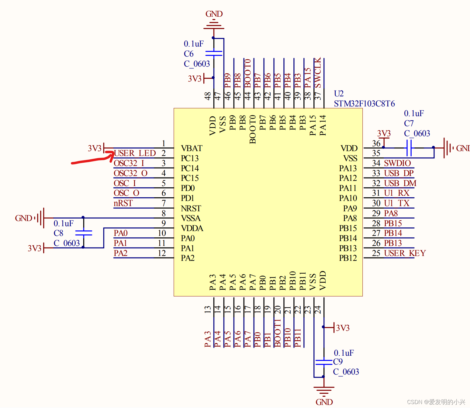
This article demonstrates basic STM32 GPIO control by blinking an onboard LED using both the Standard Peripheral Library and direct register manipulation. The target hardware uses the PC13 pin to drive the LED: a low output turns the LED on, a high output turns it off. All code is developed on an STM32F103 minimum system board.
Schematic Analysis
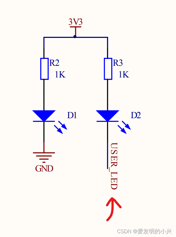
The LED is connected to PC13 through a current-limiting resistor. When the MCU drives PC13 low, current flows and the LED illuminates; driving it high stops the current and the LED turns off.
 Library-Based Implementation
The library version abstracts hardware details. The initialization configures PC13 as a push‑pull output and sets it high initially. Two helper functions toggle the LED state. The code below uses a simple delay loop built with nested for loops.
main.c``` #include "stm32f10x.h" #include "led_control.h"
void SimpleDelay(uint32_t cycles) { uint16_t outer = 0, inner = 0; for (outer = 0; outer < cycles; outer++) { for (inner = 0; inner < 65535; inner++); } }
int main(void) { LED_Config(); while (1) { LED_SetState(1); // turn on SimpleDelay(100); LED_SetState(0); // turn off SimpleDelay(100); } }
**led\_control.c**```
#include "stm32f10x.h"
#include "led_control.h"

void LED_Config(void)
{
    GPIO_InitTypeDef gpioInit;

    RCC_APB2PeriphClockCmd(RCC_APB2Periph_GPIOC, ENABLE);

    gpioInit.GPIO_Mode  = GPIO_Mode_Out_PP;
    gpioInit.GPIO_Pin   = GPIO_Pin_13;
    gpioInit.GPIO_Speed = GPIO_Speed_50MHz;
    GPIO_Init(GPIOC, &gpioInit);

    GPIO_SetBits(GPIOC, GPIO_Pin_13);   // LED off by default
}

void LED_SetState(uint8_t ledOn)
{
    if (ledOn)
    {
        GPIO_ResetBits(GPIOC, GPIO_Pin_13);  // drive low -> LED on
    }
    else
    {
        GPIO_SetBits(GPIOC, GPIO_Pin_13);    // drive high -> LED off
    }
}
led_control.h``` #ifndef __LED_CONTROL_H #define __LED_CONTROL_H
#include "stm32f10x.h"
void LED_Config(void); void LED_SetState(uint8_t ledOn);
#endif
The library approach acts as a quick template – changing a pin number requires only small modifications inside `LED_Config`.
Register-Level Implementation
-----------------------------
Understanding direct register access revealss how the microcontroller actually works. The first step is enabling the clock for GPIOC through the **APB2 peripheral clock enable register (RCC\_APB2ENR)**.
The `IOPCEN` bit (bit 4) must be set. The peripheral base address for the Reset and Clock Control (RCC) is `0x40021000`. The CMSIS header maps this to a structure pointer:
#define RCC ((RCC_TypeDef *) 0x40021000)
Thus `RCC->APB2ENR` directly accesses the memory-mapped register. Enabling the GPIOC clock:
RCC->APB2ENR |= (uint32_t)0x00000010; // set IOPCEN
Next, the pin must be configured via the **port configuration register high (GPIOx\_CRH)**. Bits 23:20 control PC13. A safe approach clears those bits first, then sets the mode to *general purpose output push‑pull, 50 MHz*.
```
GPIOC->CRH &= (uint32_t)0xFF0FFFFF; // clear bits 23:20
GPIOC->CRH |= (uint32_t)0x00300000; // push‑pull output, 50 MHz (binary 0011)
Output level control uses two registers: BSRR for setting bits and BRR for resetting bits. Writing a ‘1’ to the corresponding bit position performs the action without affecting other pins.
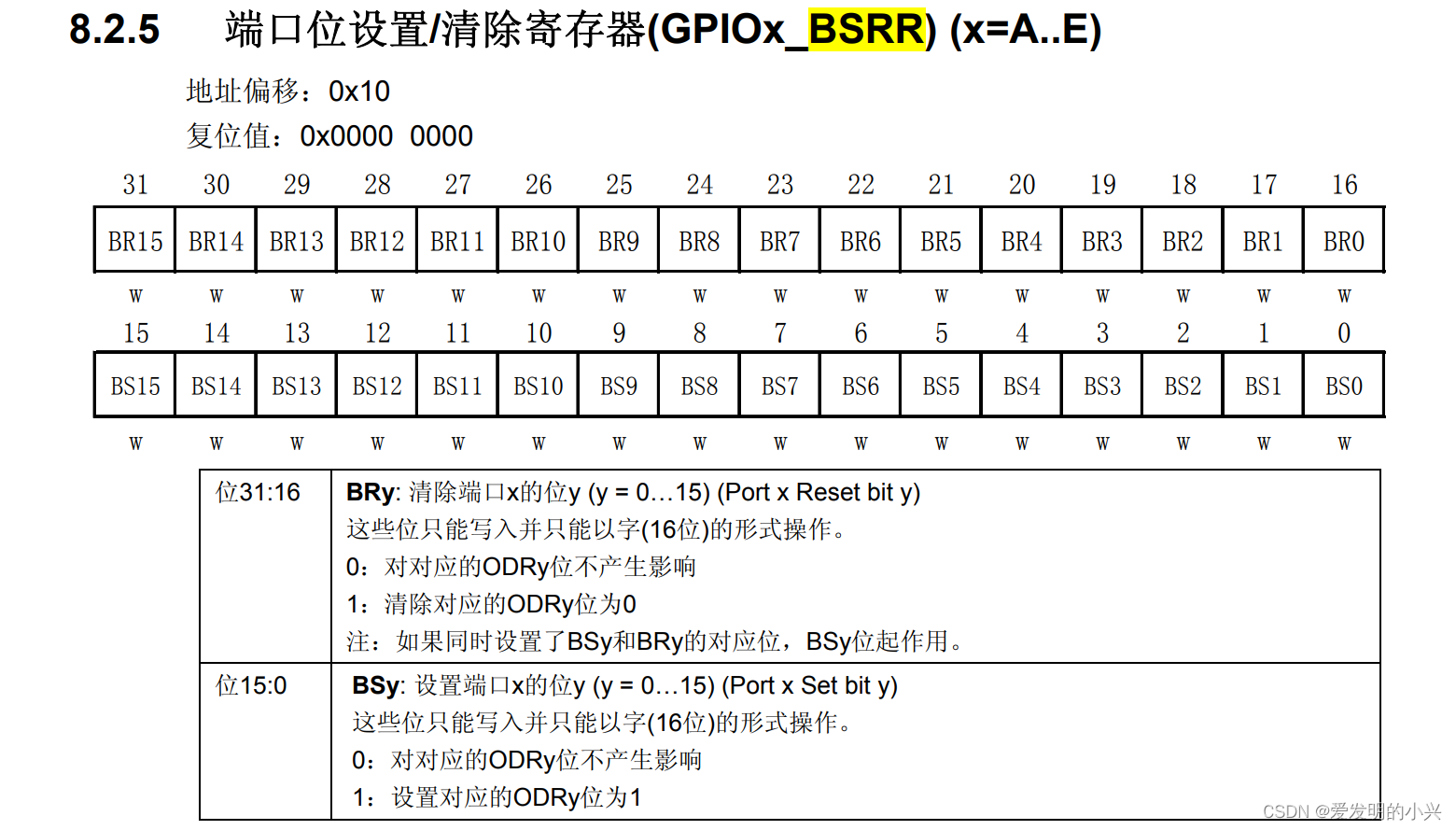
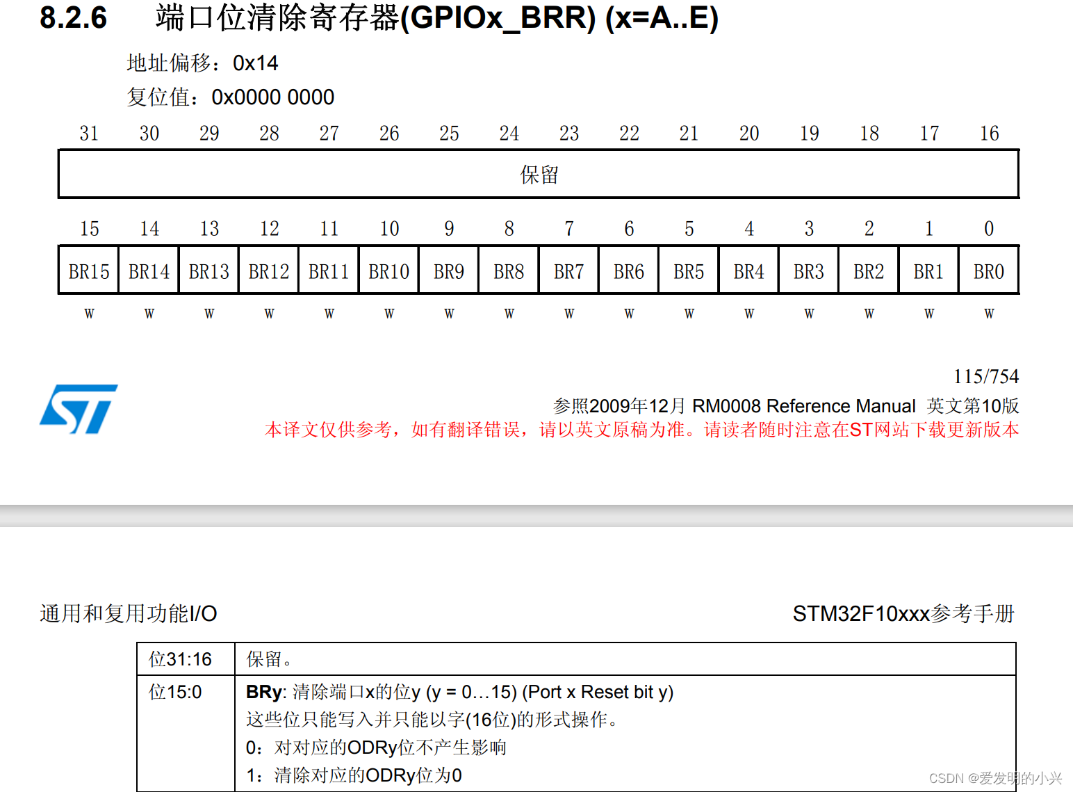 Setting PC13 high (LED off) is done by writing
 0x00002000 to BSRR; setting it low (LED on) writes 0x2000 to BRR.
A complete register-based blink program:
#include "stm32f10x.h"

void SimpleDelay(uint32_t cycles)
{
    uint16_t outer = 0, inner = 0;
    for (outer = 0; outer < cycles; outer++)
    {
        for (inner = 0; inner < 65535; inner++);
    }
}

int main(void)
{
    // Enable GPIOC clock
    RCC->APB2ENR |= (uint32_t)0x00000010;

    // Configure PC13: push‑pull output, 50 MHz
    GPIOC->CRH &= (uint32_t)0xFF0FFFFF;
    GPIOC->CRH |= (uint32_t)0x00300000;

    while (1)
    {
        GPIOC->BSRR = (uint32_t)0x00002000;   // LED off (high)
        SimpleDelay(100);
        GPIOC->BRR  = (uint16_t)0x2000;       // LED on  (low)
        SimpleDelay(100);
    }
}
GPIO Characteristics Overview
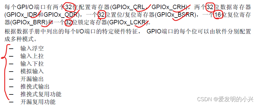
The STM32 GPIO peripheral is highly flexible, supporting multiple input, output, and alternate function modes.
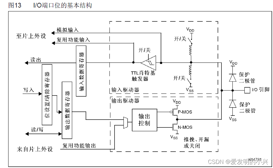
 ### Pin Internal Structure
 ### Input Modes
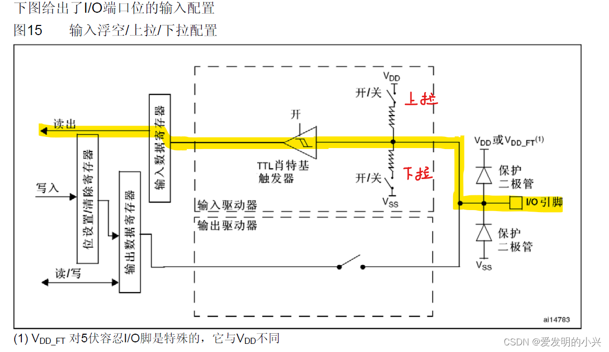
Input floating, input pull‑up, and input pull‑down modes are selected through the configuration registers. The diagrams show the path from the I/O pad to the input data register.

 ### Output Modes
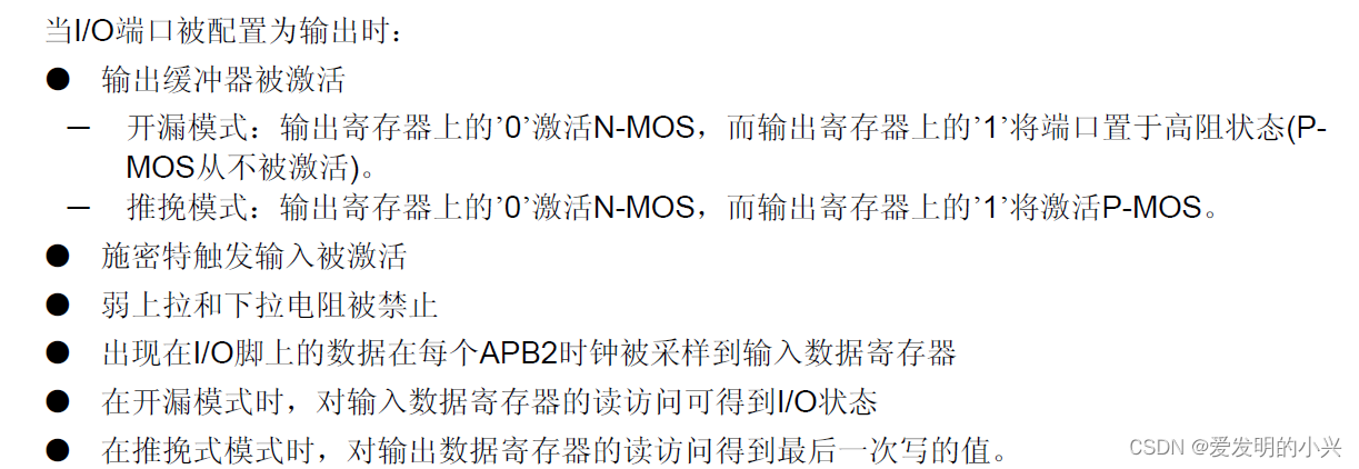
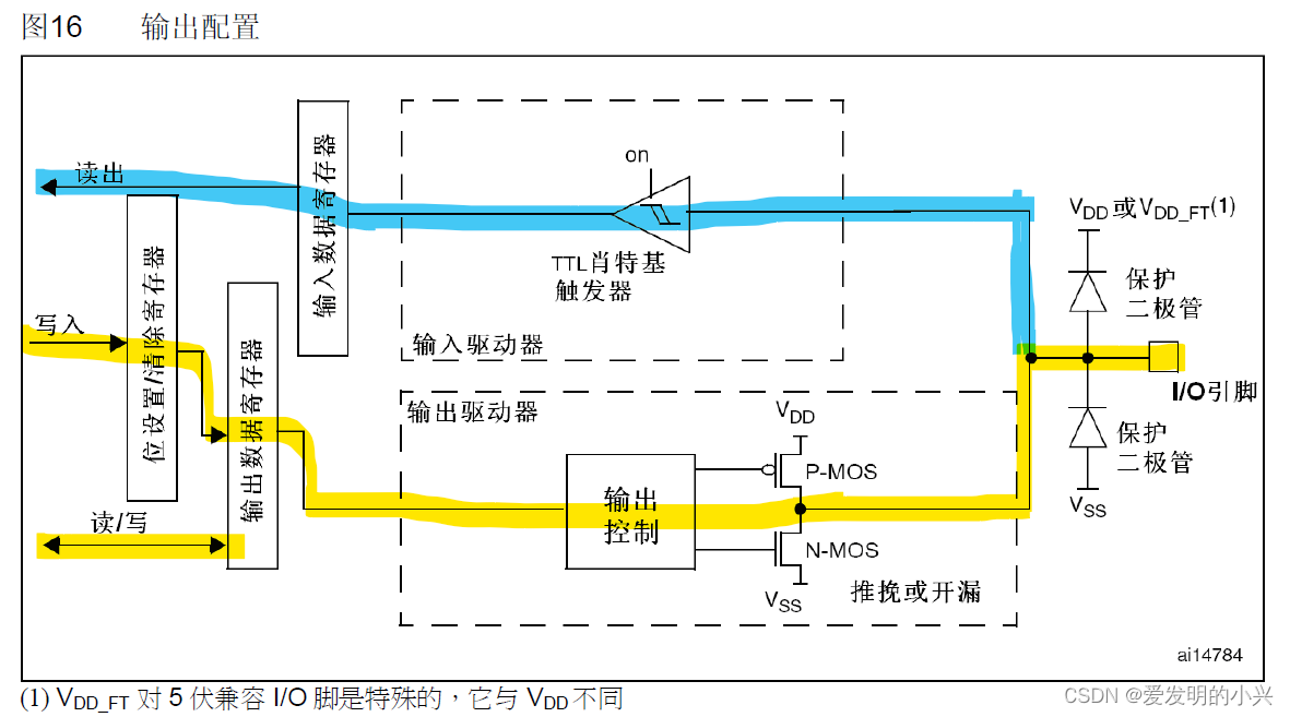
Push‑pull and open‑drain output modes are available. In push‑pull mode the pin can actively drive both high and low levels.
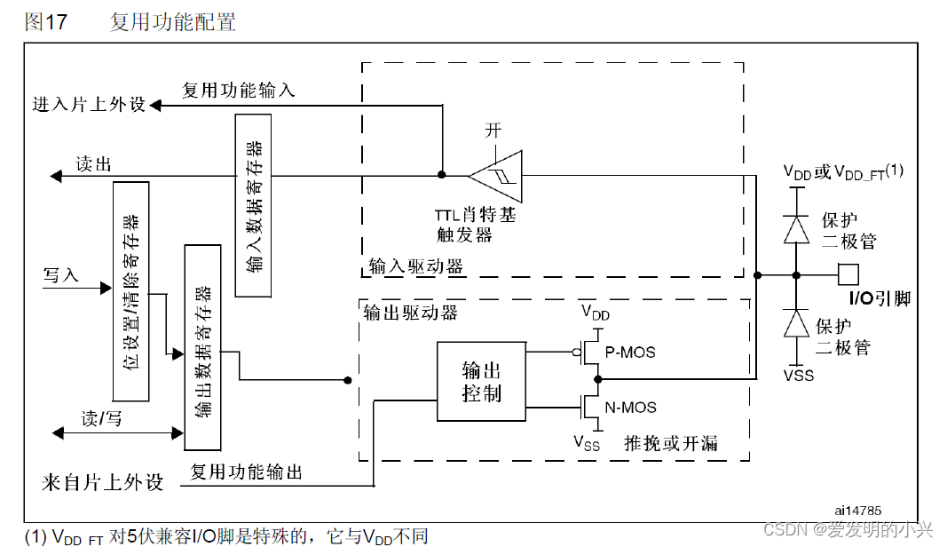
 ### Alternate Function Modes
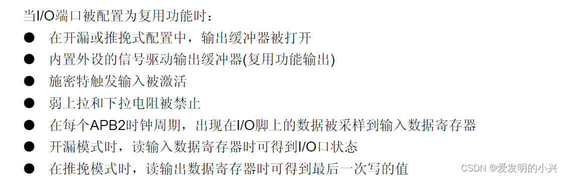
Peripheral functions (USART, SPI, timers, etc.) can be multiplexed onto GPIO pins. The pin is internally rerouted to the specific peripheral.
 ### Analog Mode
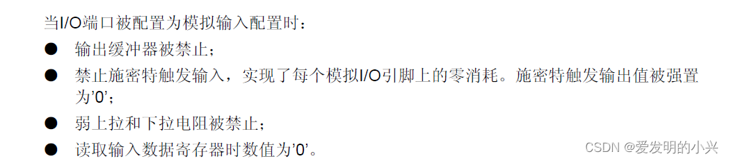
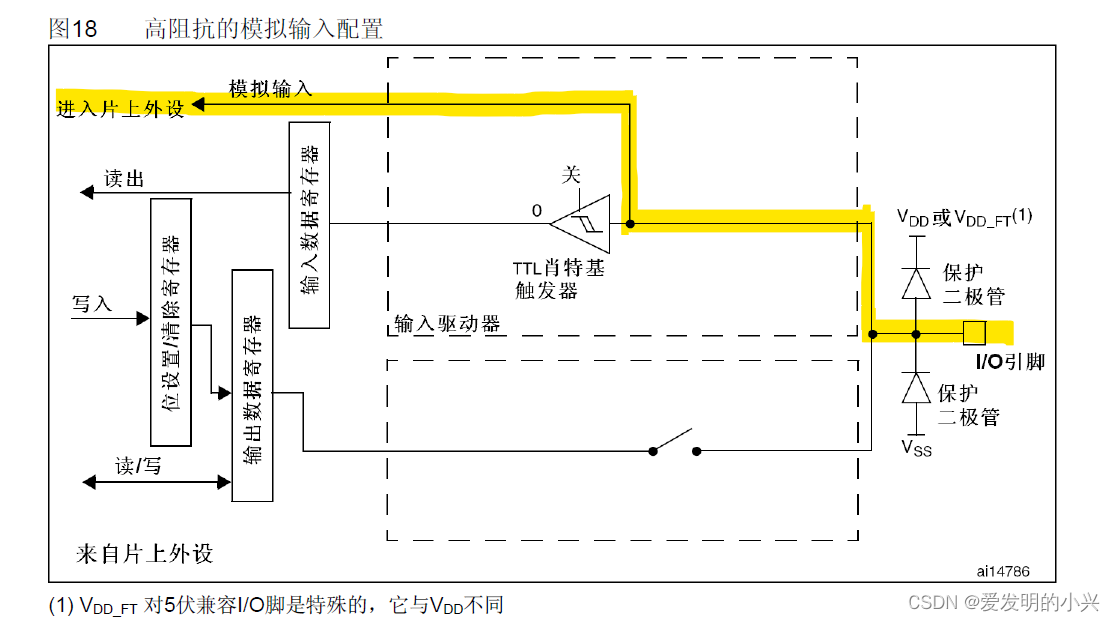
For ADC inputs, the pin is disconnected from the digital input buffer to reduce noise.