1. Verilog Design
This experiment implements a three‑stage CIC decimation filter with a decimation factor of 64. Recalling the CIC filter structure discussed previously, the hardware is straightforward: integrators are built with adders and D flip‑flops, the downsampler uses a clock divider, and comb stages are formed by subtractors and flip‑flops.
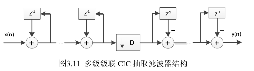
First we design a clock divider. Its input are the main clock clk and an active‑low reset rst_n; the output is a div_clk signal running at 1/64 of the input frequency.
A counter‑based approach is used. While reset is low, the counter and output are cleared. When reset goes high, the counter increments on each rising edge of clk. The divider can be implemented with a 6‑bit counter that counts from 0 to 63 and toggles div_clk when the count reaches 31. This gives a symmetrical 64‑cycle period.
The Verilog code for the redesigned divider is shown below:
module clock_divider(
    input wire clk,
    input wire rst_n,
    output reg div_clk
);

    reg [5:0] tick_counter;

    always @(posedge clk or negedge rst_n) begin
        if (!rst_n) begin
            tick_counter <= 6'd0;
            div_clk       <= 1'b0;
        end else begin
            if (tick_counter == 6'd63)
                tick_counter <= 6'd0;
            else
                tick_counter <= tick_counter + 1'b1;

            if (tick_counter == 6'd31)
                div_clk <= ~div_clk;
        end
    end

endmodule
Next we implement the CIC filter itself. It accepts clk, rst_n, a 1‑bit modulator input data_in, and provides a 19‑bit output data_out.
The integrator stages increase the data width. The required output bit width is computed with
The comb stages operate on the downsampled side and must be clocked by the divided clock div_clk.
The CIC filter Verilog code, with renamed modules and signals, follows:
module cic_decimator(
    input wire clk,
    input wire rst_n,
    input wire data_in,
    output wire [18:0] data_out
);

    reg  [18:0] out_reg;
    wire        div_clk;
    reg  [18:0] int1, int2, int3;
    wire [18:0] int1_next, int2_next, int3_next;

    // Integrator adders
    assign int1_next = int1 + data_in;
    assign int2_next = int2 + int1;
    assign int3_next = int3 + int2;

    // Integrator registers
    always @(posedge clk or negedge rst_n) begin
        if (!rst_n) begin
            int1 <= 19'b0;
            int2 <= 19'b0;
            int3 <= 19'b0;
        end else begin
            int1 <= int1_next;
            int2 <= int2_next;
            int3 <= int3_next;
        end
    end

    // Clock divider instantiation
    clock_divider clk_div_inst (
        .clk    (clk),
        .rst_n  (rst_n),
        .div_clk(div_clk)
    );

    reg  [18:0] comb1, comb2, comb3;
    wire [18:0] comb1_next, comb2_next, comb3_next;

    // Comb subtractors
    assign comb1_next = int3_next - comb1;
    assign comb2_next = comb1_next - comb2;
    assign comb3_next = comb2_next - comb3;

    // Comb registers (downsampled clock domain)
    always @(posedge div_clk or negedge rst_n) begin
        if (!rst_n) begin
            comb1 <= 19'b0;
            comb2 <= 19'b0;
            comb3 <= 19'b0;
        end else begin
            comb1 <= int3_next;
            comb2 <= comb1_next;
            comb3 <= comb2_next;
        end
    end

    // Output register
    always @(posedge div_clk or negedge rst_n) begin
        if (!rst_n)
            out_reg <= 19'd0;
        else
            out_reg <= comb3_next;
    end

    assign data_out = out_reg;

endmodule
A testbench is provided to verify the design. The file 1k1000mv.txt contains a bitstream from a sigma‑delta modulator sampling one period of a sine wave. The testbench uses $readmemb to load this data into a memory array and sequentially feeds it to the filter input data_in. The system clock period is set to 156.25 ns, and the reset is released 500 ns after simulation starts.
The testbench code is given below:
`timescale 1ns/1ns
`define HALF_PERIOD 78.125

module tb_cic_filter;
    reg clk, rst_n, data_in;
    wire [18:0] data_out;

    // Generate 156.25 ns clock
    always #`HALF_PERIOD clk = ~clk;

    // Initial reset and clock
    initial begin
        clk   = 1'b0;
        rst_n = 1'b0;
        #500;
        rst_n = 1'b1;
    end

    integer idx;
    reg bitstream [0:3000000];

    // Load modulator bitstream
    initial $readmemb("1k1000mv.txt", bitstream);

    // Stream data into the filter
    always @(posedge clk or negedge rst_n) begin
        if (!rst_n) begin
            idx     = 0;
            data_in = 1'b0;
        end else begin
            data_in = bitstream[idx];
            idx     = idx + 1;
        end
    end

    // Unit under test
    cic_decimator uut (
        .clk      (clk),
        .rst_n    (rst_n),
        .data_in  (data_in),
        .data_out (data_out)
    );

endmodule
2. Pre‑simulation with ModelSim
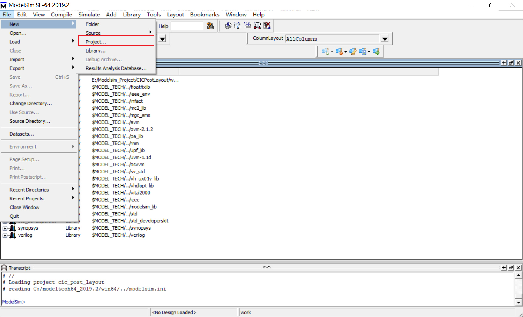
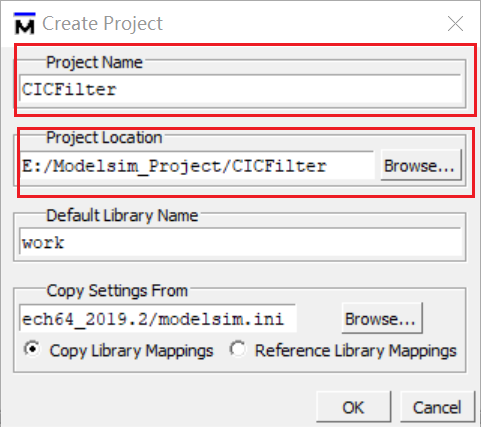
1. Launch ModelSim. Create a new project via File → New → Project.... Name it CICFilter and set the project location.
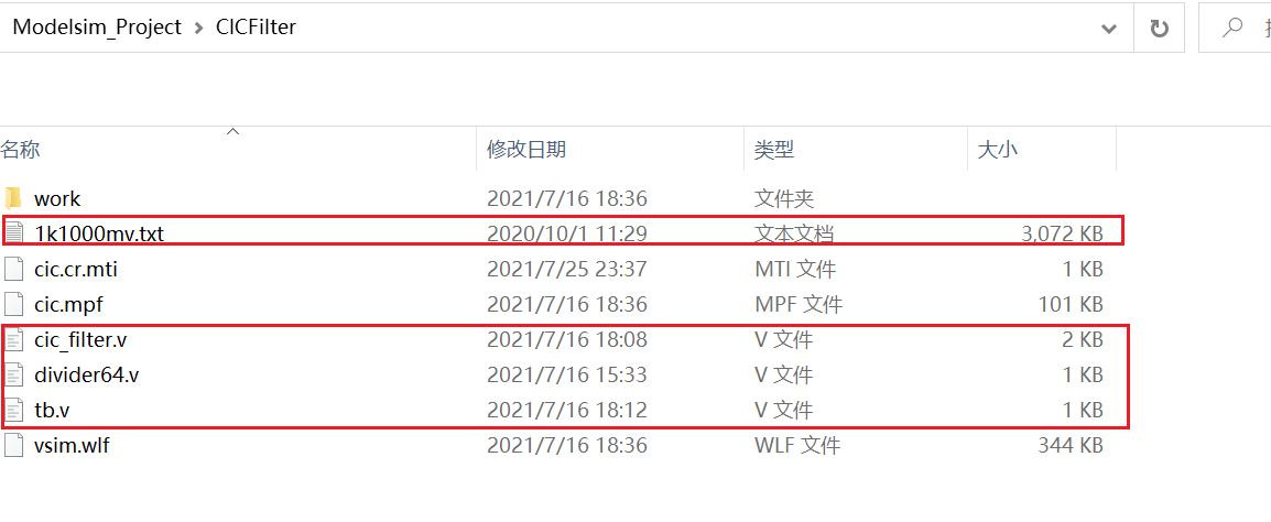
2. Place all Verilog source files and 1k1000mv.txt into the project directory.
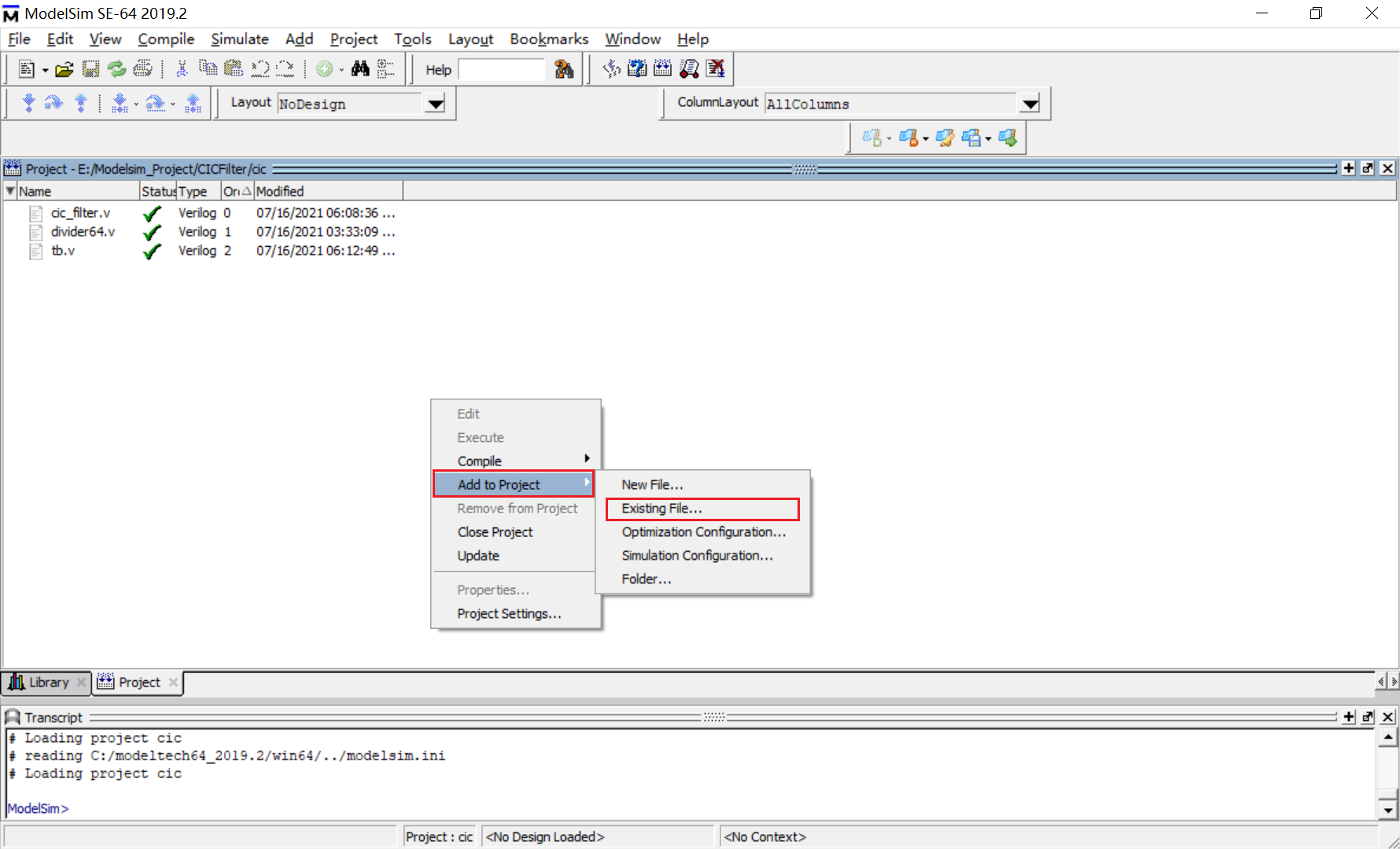
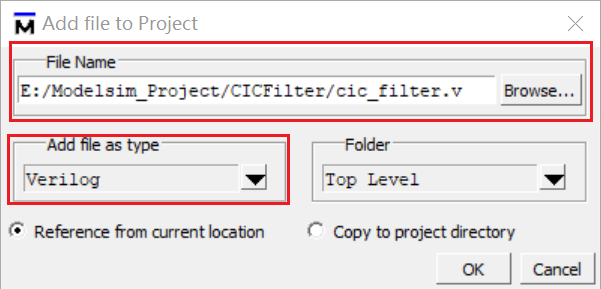
3. In the Project tab, right‑click and select Add to Project → Existing File.... Choose the Verilog files, set Add file as type to Verilog, and add all three files.
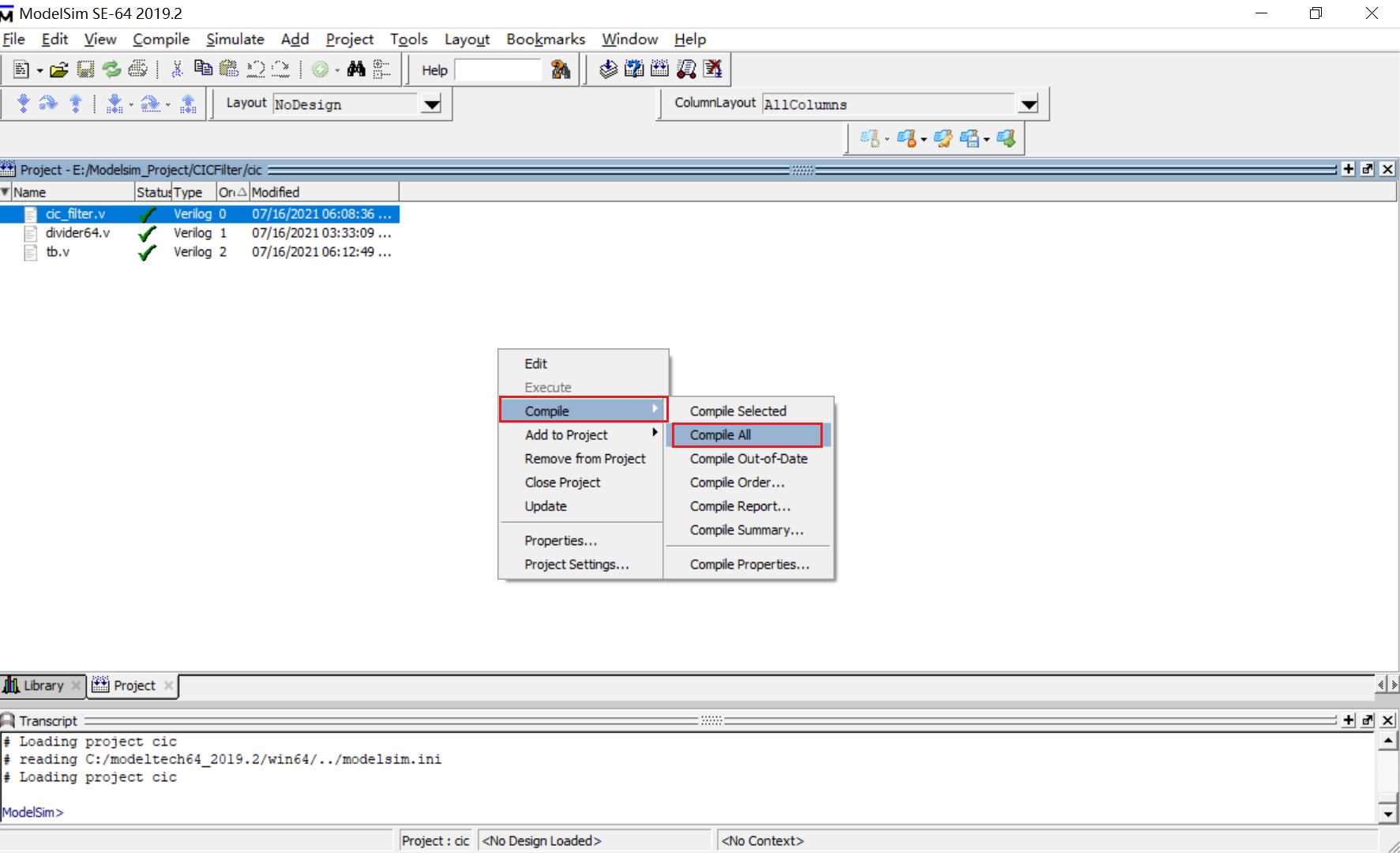
4. Right‑click in the Project tab again and choose Compile → Compile All.
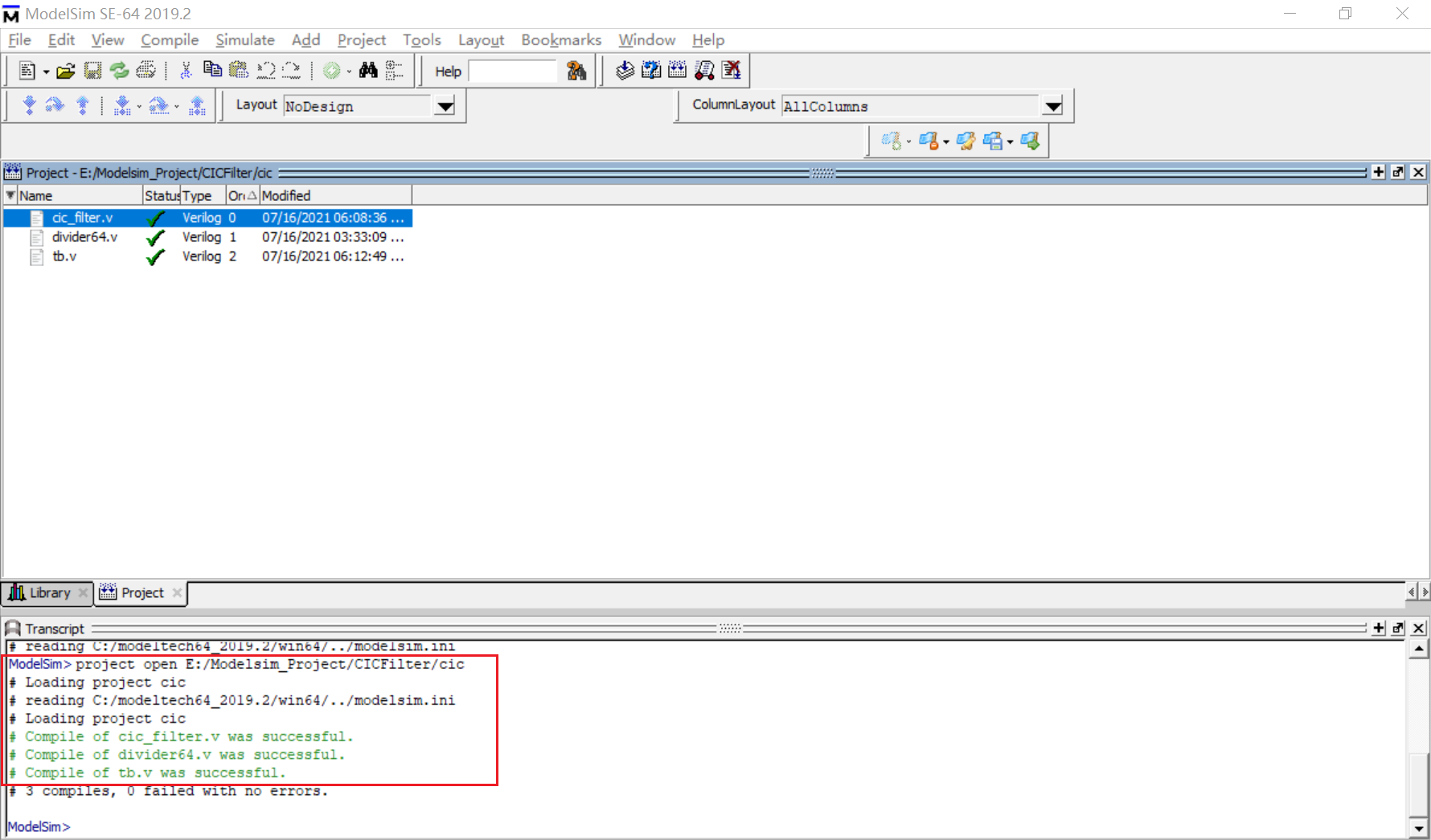
5. A successful compilation is reported in the Transcript window. If errors appear, fix the Verilog and recompile.
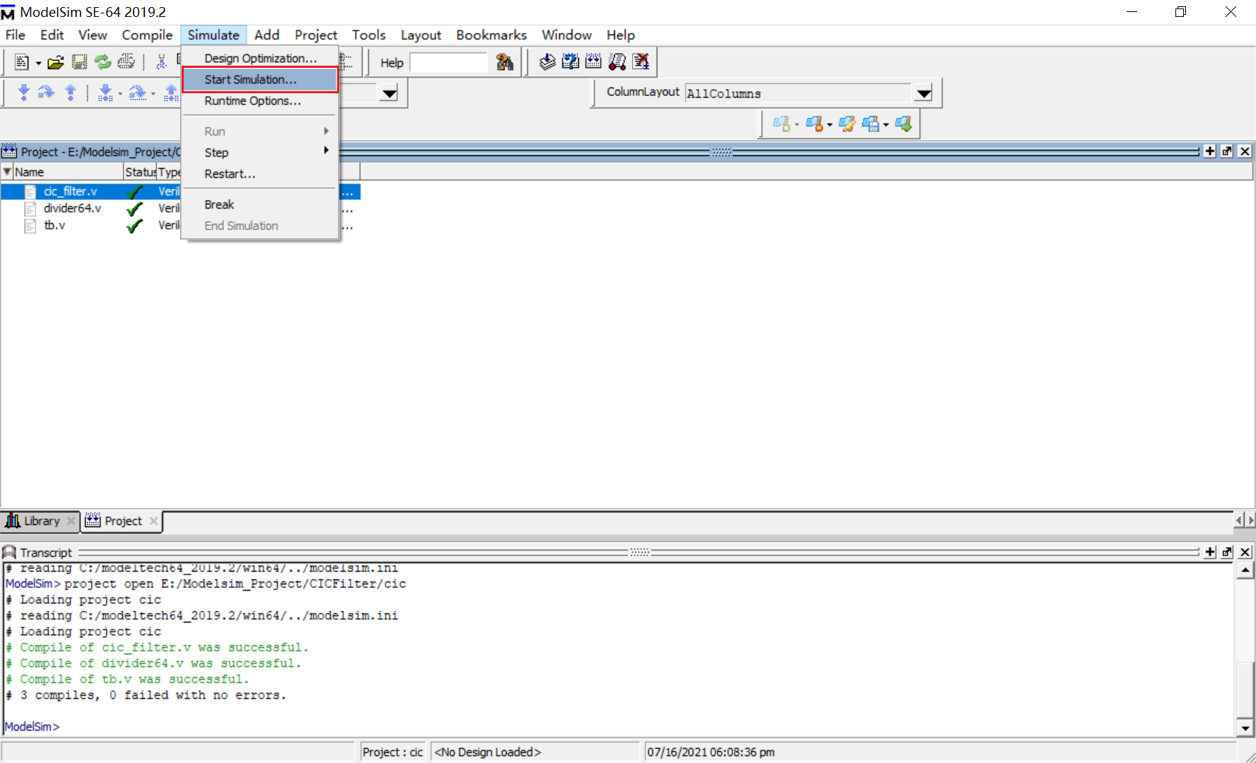
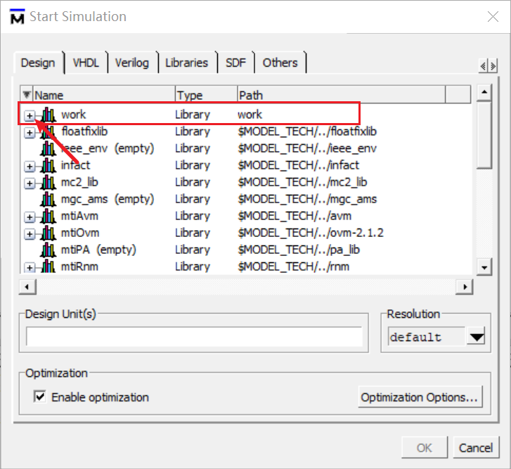
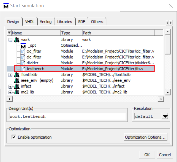
6. Start the simulation with Simulate → Start Simulation.... Expand the work library, select tb_cic_filter, and click OK.
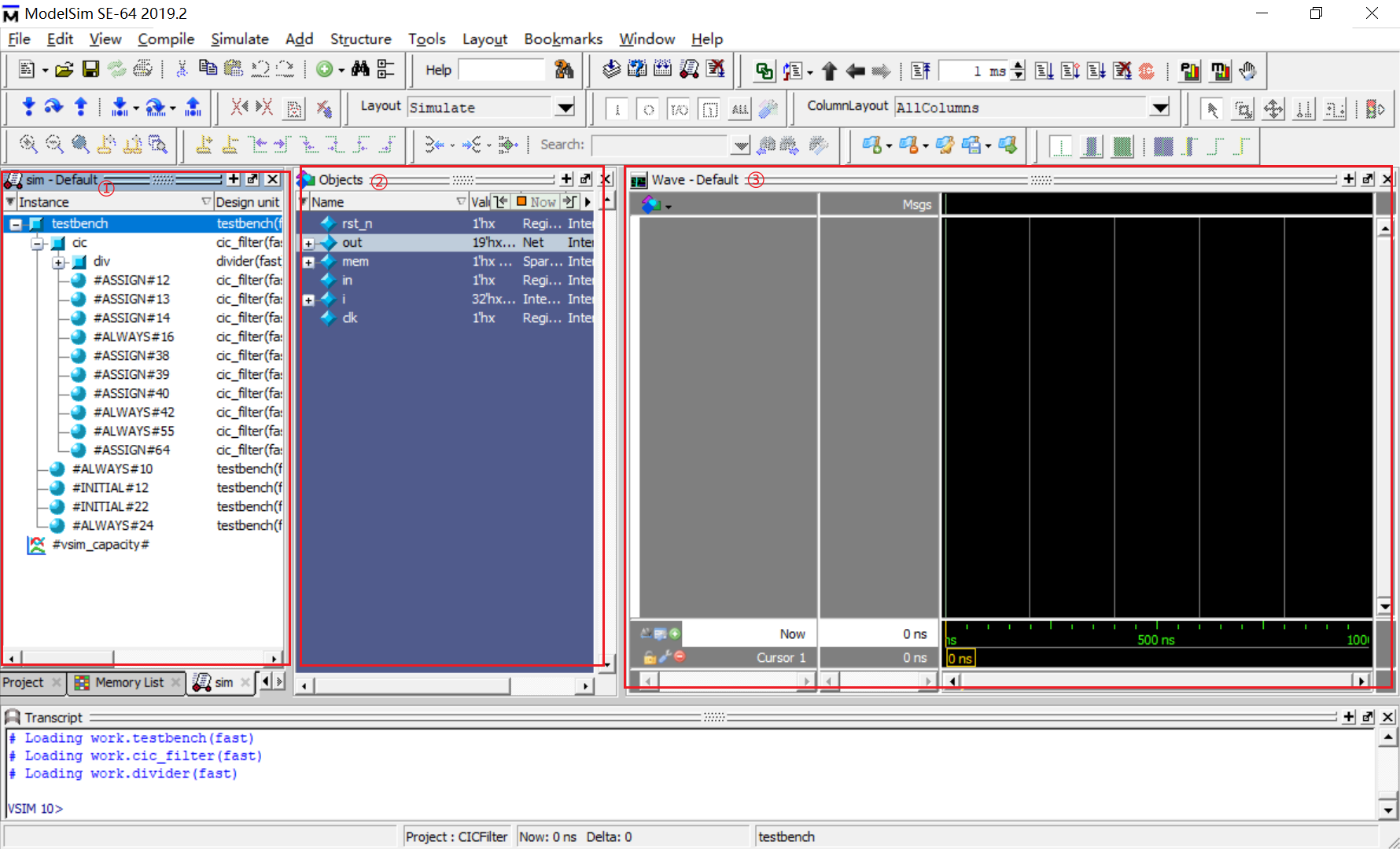
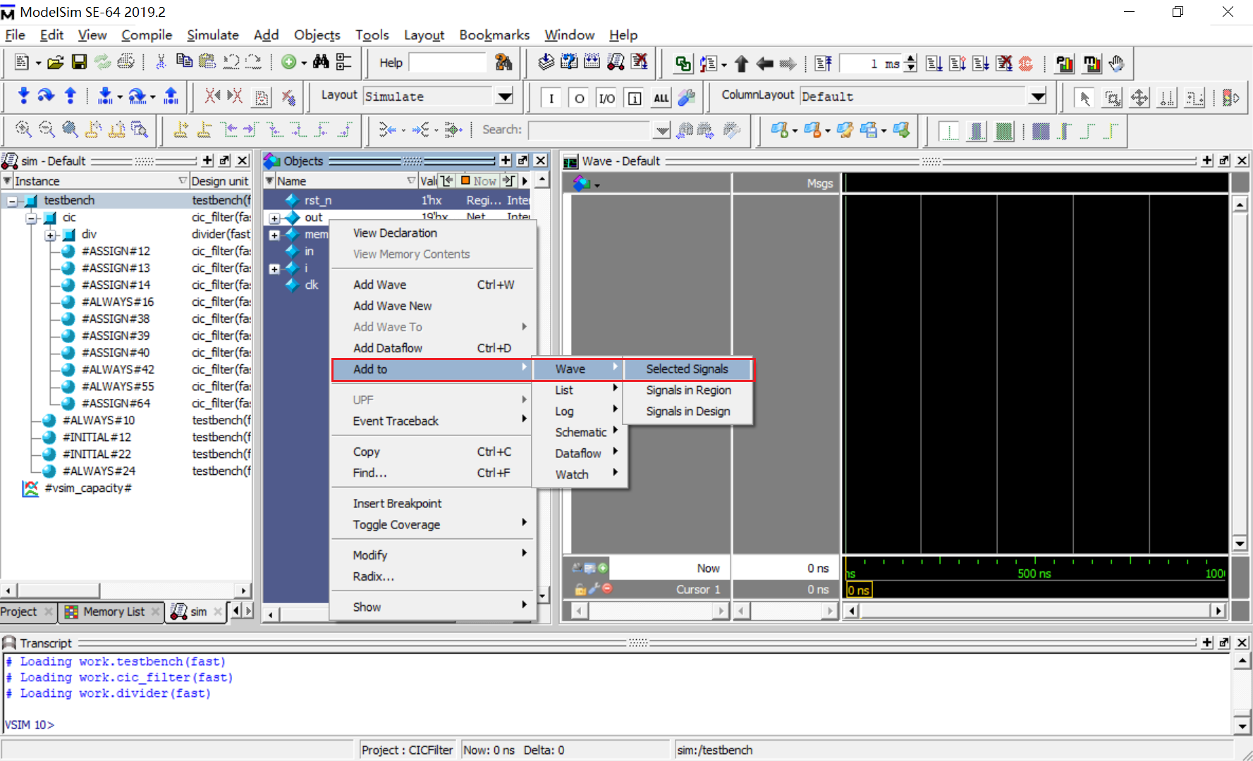
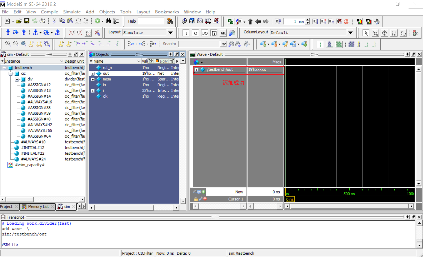
7. In the simulation environment, the Instance pane (①) lists all instantiated modules; the Objects pane (②) shows signals, registers, and memories of the selected module; the Wave pane (③) displays waveforms. Select tb_cic_filter in the Instance pane, right‑click data_out in the Objects pane, and choose Add to → Wave → Selected Signals.
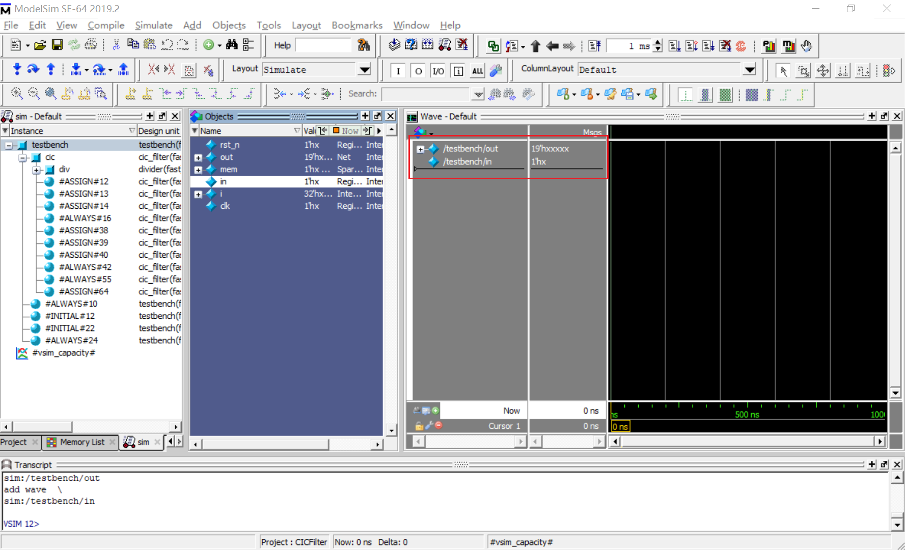
8. Similarly add data_in to the Wave window.
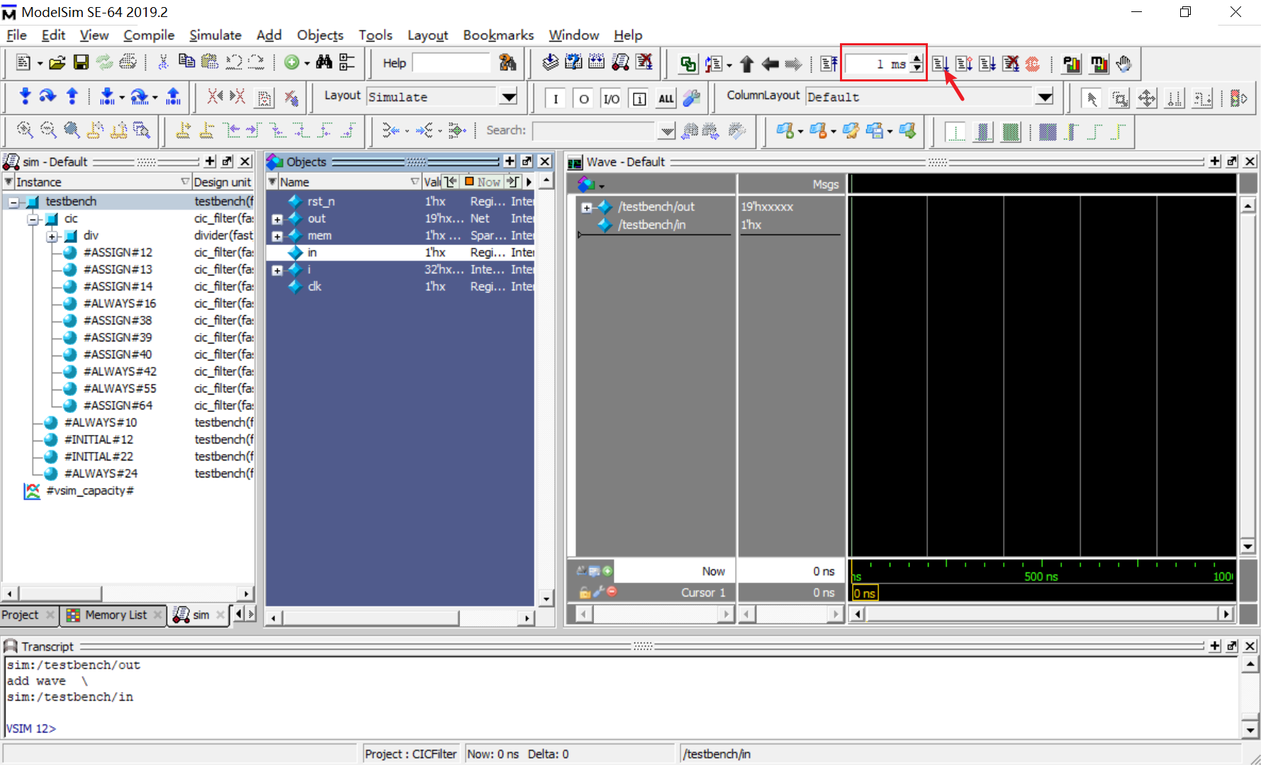
9. Set the simulation time to 1 ms in the toolbar and click the Run icon.
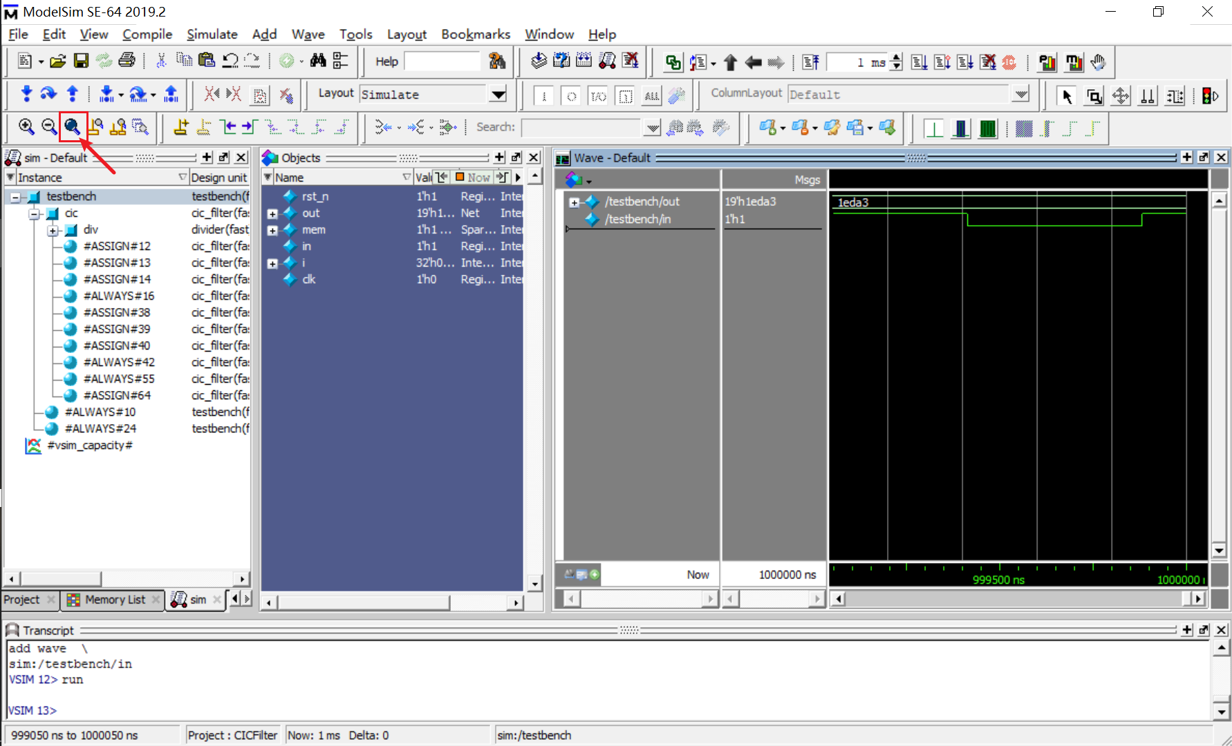
10. Waveforms appear in green. Click the zoom‑fit icon to adjust the time axis.
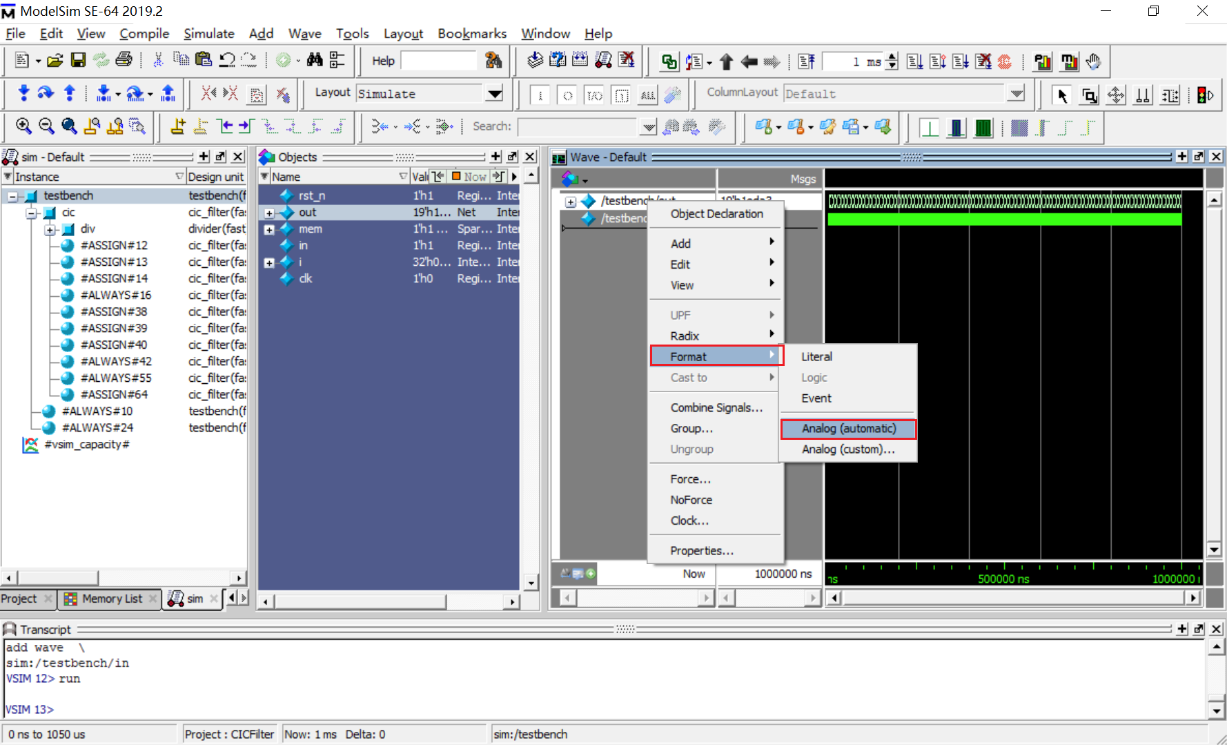
11. Right‑click the data_out signal in the Wave window, then Format → Analog (automatic).
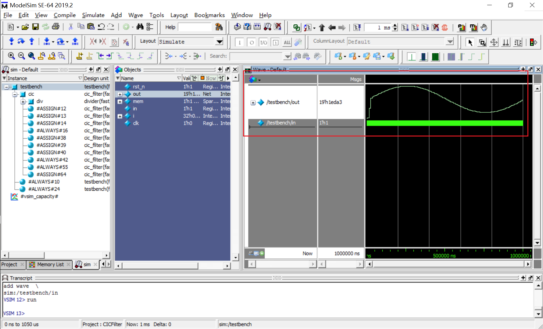
12. A single period of a sine wave becomes visible.
13. Continue running the simulation to see multiple sine periods.
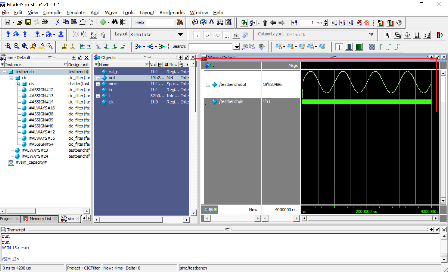
14. Zoom in on the time axis. It can be observed that when data_out is large (wave crest), data_in is dominated by 1s; when data_out is small (wave trough), data_in is dominated by 0s. This matches the expected relationship between the modulator bitstream and the CIC filter output.
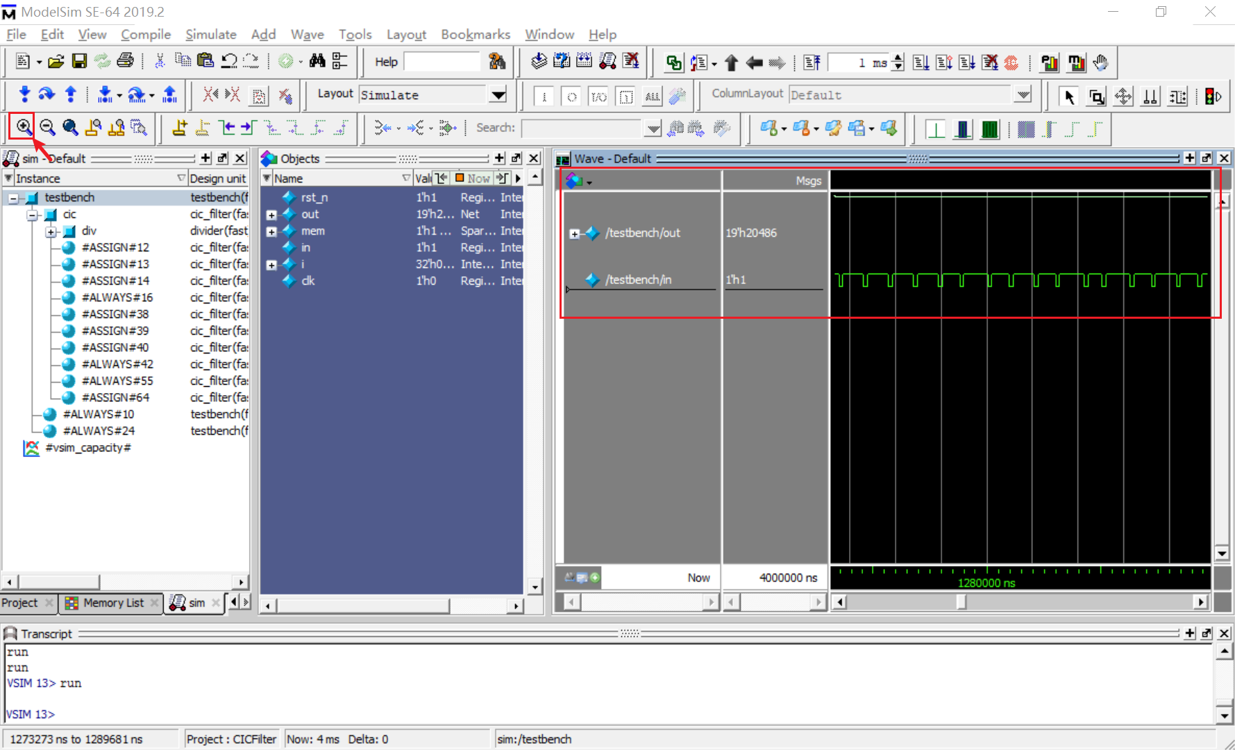
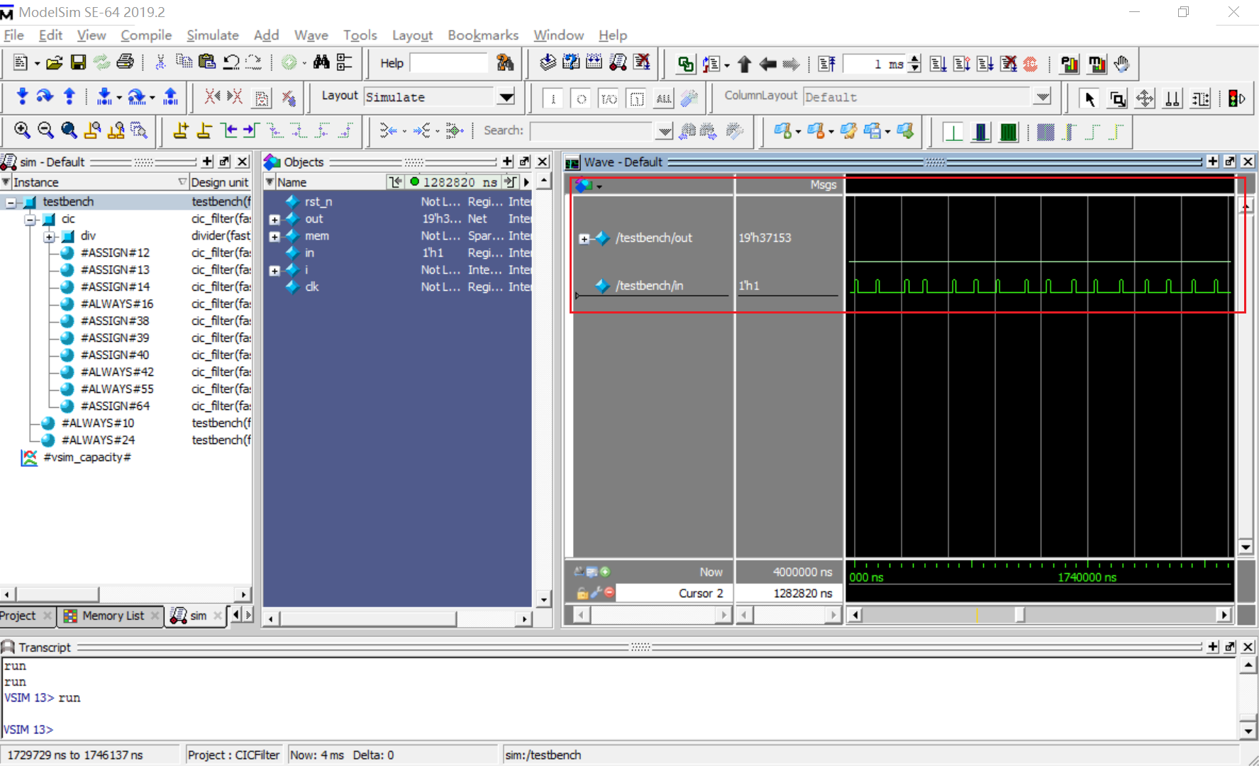
The Verilog implementation and pre‑simulation of the CIC filter are now complete.
3. References
https://blog.csdn.net/FPGADesigner/article/details/80885415
Introduction to Digital IC Design – From HDL to Layout, Yu Dunshen, Department of Microelecrtonics, Peking University.